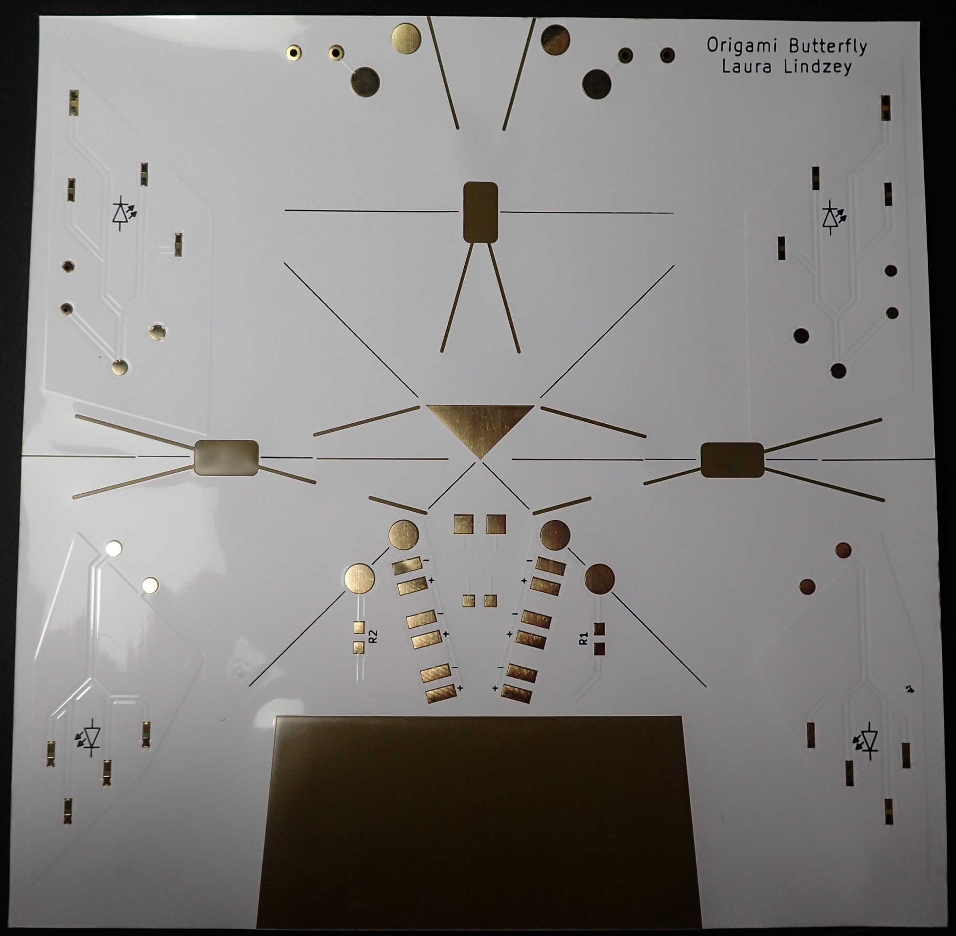
Origami Butterfly: Adventures with Flexible PCB
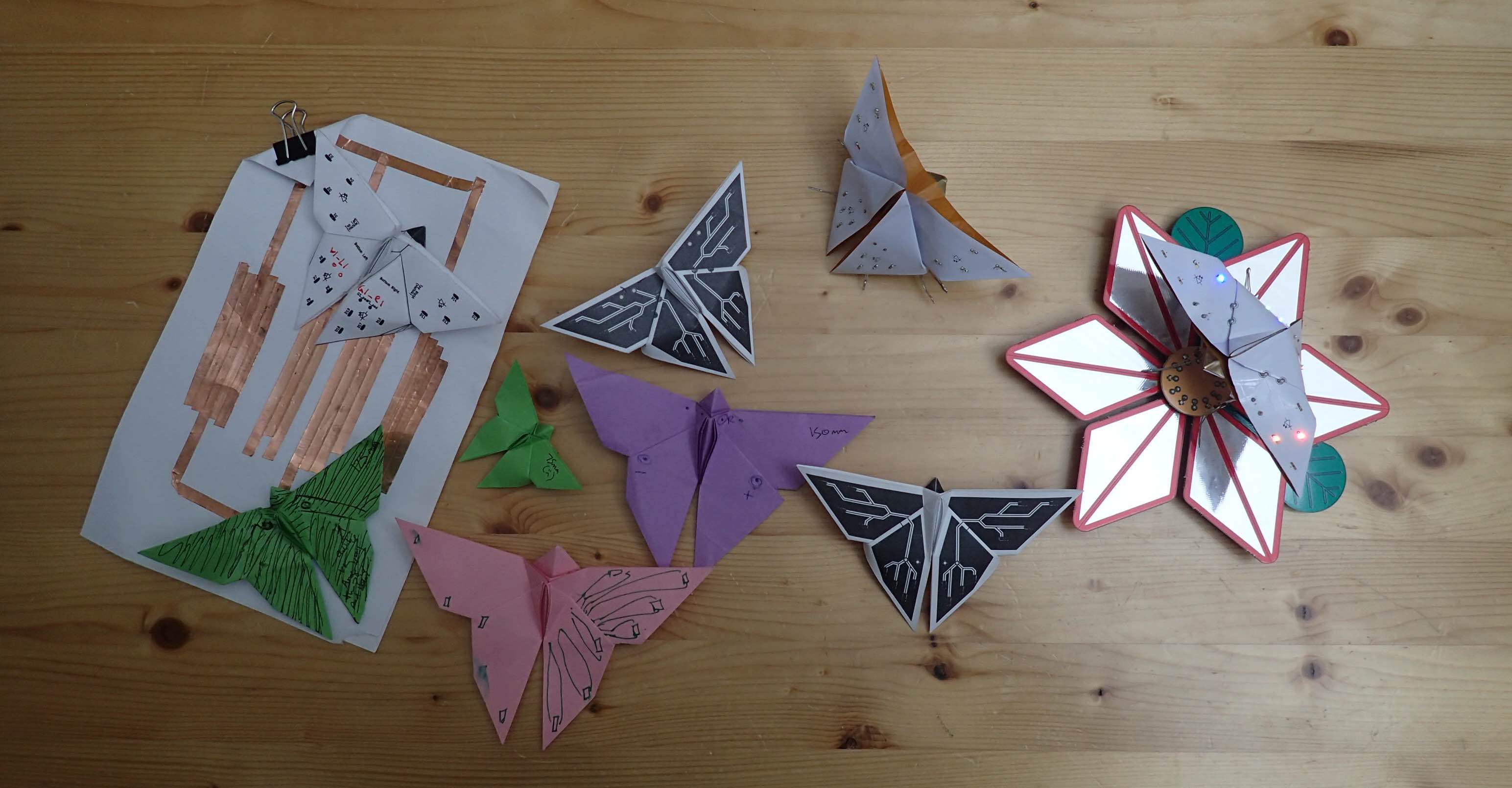
A very partial set of butterfly and flower prototypes. It turns out that origami butterflies have a natural predator in housecats, and I found ripped-apart wings all over the place.
As soon as I learned that I could order flexible PCBs, I knew I wanted to play with designing “origami circuits”, where the board itself is folded and soldered into a sculpture. A PCB exchange organized by a group of Boldport Club members gave me the perfect excuse to iterate on a concept and ship it out to an appreciative audience. My goal for this post is to answer some of past-Laura’s questions about what working with flexible PCB is like (OK, OK, and to show off the final product…)
The origami butterfly that I learned as a child1 seemed like a simple enough fold pattern to be a good candidate. But what should I design a circuit to do? And how should I power it? While I could have attached a coin cell battery, that seemed clunky. Butterflies don’t need weights!
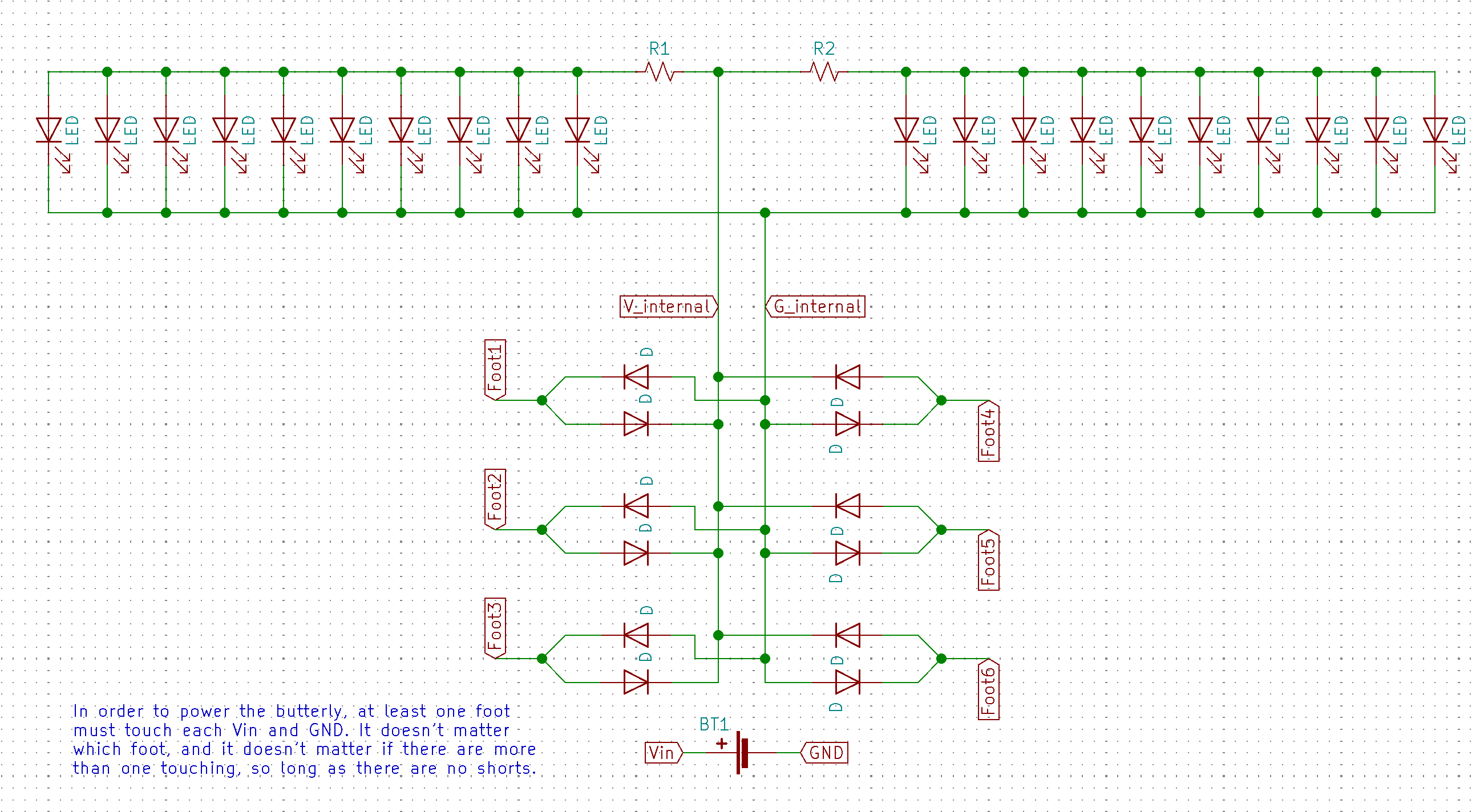
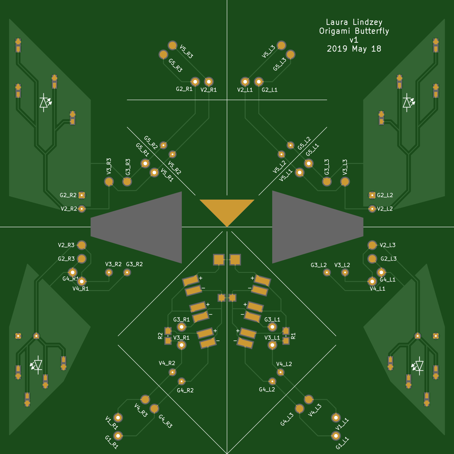
Schematic for the butterfly’s circuit, laid out in KiCAD
Brainstorming with my partner, we came up with the idea of a “power flower”, where the butterfly would alight to get power. I realized that if I made the butterfly’s legs out of diodes2, they could be arranged in a way that it doesn’t matter which legs land on positive/negative pads, so long as at least one of each is contacted and there aren’t any shorts. With that interaction, I didn’t think it needed any cooler circuit than to just light up when on the flower, so I was all set for a concept!
I prototyped a LOT with pen on paper. How big (and thus $$) did the board really need to be? How should I route traces? What looked good for LED layout? For laying out the actual PCB, I used KiCad, manually adjusting footprint locations and fold pattern guidelines based on my prototypes. The trickiest bit was making sure that all of the holes and pads aligned when folded.
Material Properties
When I was designing the first PCB prototype, I had no idea how well the flexible material would take a crease, which is more than a little important for origami.
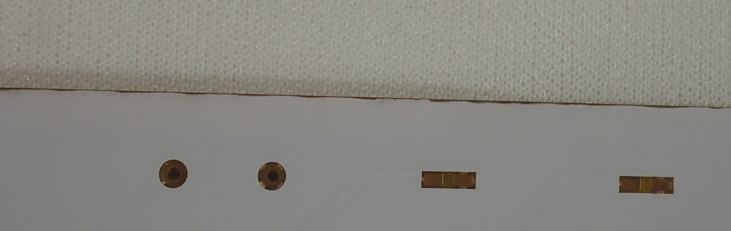
I went with single layer 0.1mm boards3 with white coverlay4, ordered from PCBWay. According to my calipers, my printer paper is ~0.09 mm thick, and I have no trouble folding it, so I figured that at least the thickness wouldn’t be the issue.
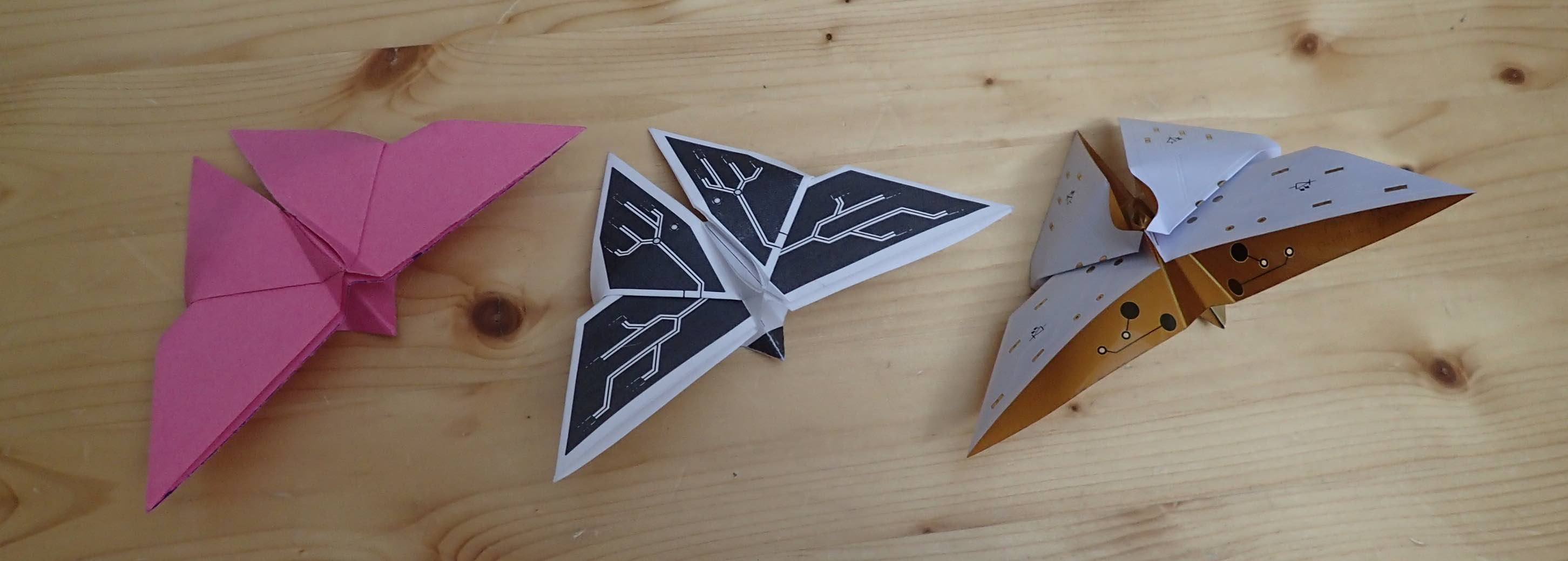
Comparison of butterfly with different materials. Origami paper (left) keeps the final shape nicely, and printer paper (center) is barely worse. The PCB butterfly (right) wants to spring apart; via and pad placement will allow solder to hold it together.
On its own, the polyimide is significantly thinner than the polyimide+coverlay combo. Additionally, it seems to hold a crease a bit better. (The coverlay makes it springier.) So, on V3, I tried to remove coverlay from as many creases as possible.
But what about brittleness? It turned out that I was a lot more worried about this than necessary:
-
V1 and V3 included creases over regions of only polyimide, and I haven’t yet observed cracking there.
-
I have had cracking around the butterfly’s head, at the boundary of a polyamide+copper+gold / polyimide+coverlay region. This is almost undetectable on the final assembled butterfly. I have not experimented to see if this is more due to the edge of the copper pour or due to the tightness of that crease.
That’s not to say that it’s EASY to fold this stuff…it’s slippery and springy.
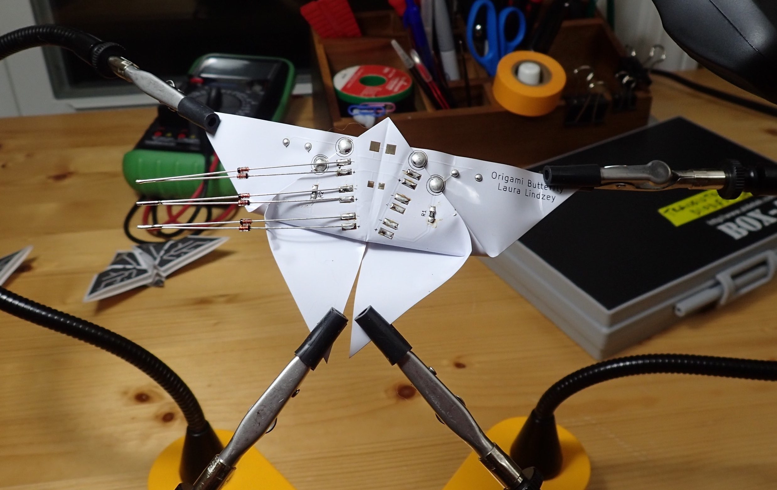
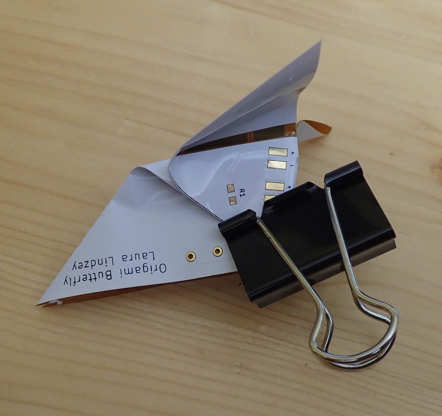
Assembling the butterfly...(left) Using quadhands to hold the butterfly while attaching legs. (right) Using a binderclip to help make the wing creases crisper.
I strongly recommend having helping hands (or quadhands), paperclips, and binderclips handy.
Design rules for flexible PCBs?
As a hobbyist, I found design guidelines for flexible PCB to be opaque to non-existent. This is in contrast to the standard FR4 boards where various fabs clearly publish their capabilities.5 Based on my obsessive googling before eventually deciding to just jump in with an order:
- Oshpark states that they use soldermask rather than coverlay on their flexi boards because their customers don’t typically have the tools to design a board that’s suitable for coverlay. (But what are the constraints?) Additionally, they couldn’t do purple soldermask because it was too brittle and cracked on flex.
- Somewhere I found the hint that coverlay can’t handle super thin lines separating pads, so for a small-enough IC, you’d have to design a rectangle masking out all of the pads, rather than individual masks per pad. I also found the info that you want the mask boundary to be larger for coverlay than for soldermask because the adhesive will be squeezed out. (But how much larger?)
- There’s lots of guidance that traces shouldn’t be routed across bends, but I couldn’t find information on exactly how bad it is / ideal curvature radii / repeated vs. static bends. Let’s just say that the one bend I have a trace going over is significantly smaller than any static radius I found mooted as OK, and routing over a sharp fold would be 5-10x smaller radius.
So … if you have a better guide for what’s possible to fabricate in the typical flexible PCB process, please let me know! Fortunately/unfortunately, I suspect that best practices for reliability in the face of flexing are going to assume many more 9’s of reliability than I care about.
Routing Traces
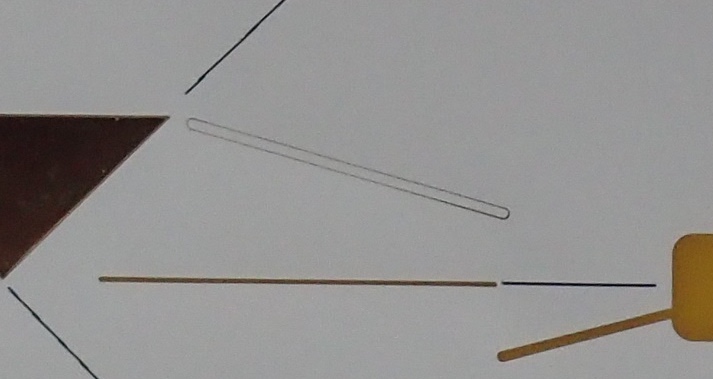
For the project I had in mind, a critical component of the design was how to route traces between different facets of the origami butterfly. The generally-agreed-upon guidance to not route traces across sharp folds made me cautious, so I tried to design a more reliable way to connect the power source on the body with the LEDs on the wings.
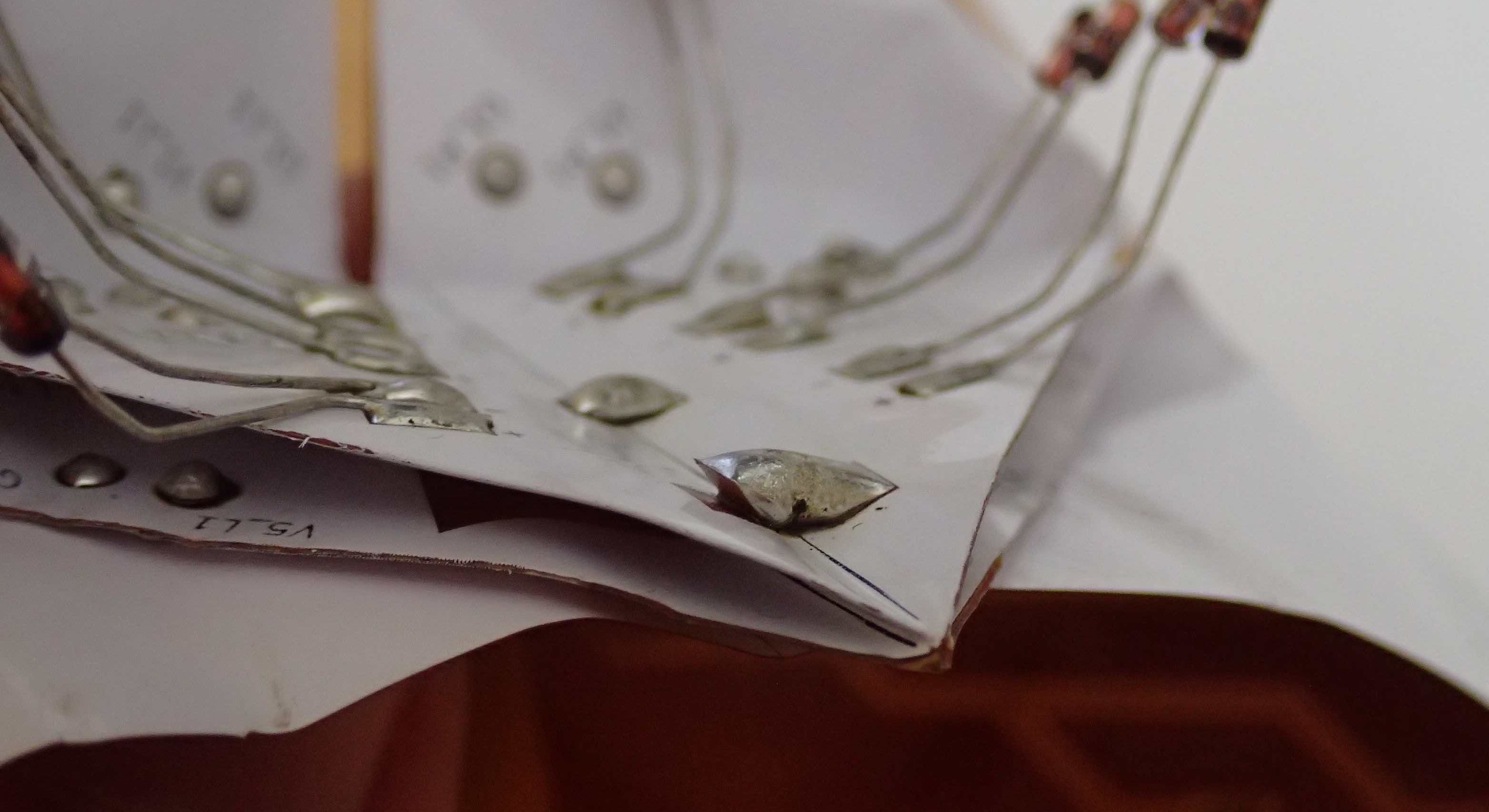
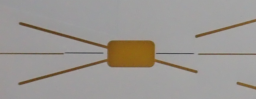
V1 made liberal use of via-equivalents. In the same way that a via connects a trace on two layers of a board, I placed through-hole footprints in two locations on the board that would overlap when the PCB was folded, and used solder blobs on both pads to form an electrical connection. In some cases, I added a third layer of connectivity using an exposed pad.
This … worked. It was also incredibly fiddly to assemble. Lessons:
- Aligning all three layers is hard. I could reliably get 2, but getting the connection with the 3rd was flaky and led to lots of debugging with a multimeter.
- It is stupidly easy to lift pads on a flexi board when re-working. Be careful with overheating!!
- It would have been easier if it was a two-layer board, so there was metal on both sides of the through-holes. It might have been possible to order it with a very minimal, metal-only back layer...
- Polyimide is an impressive thermal insulator. If you’re careful, your finger can be separated from the iron by 2-3 layers of it and not get burned immediately (it does heat up after a few seconds). This is useful when trying to get as-flat-as-possible joins.
Watching somebody else assemble my board, I realized that a better option was to use exposed pads on the edges of folds to connect multiple layers.
This was a dramatic simplification of the design, making it much more forgiving of less-precise folds AND requiring fewer solder joints. Phew.
I possibly could have designed this in a way that didn’t have any solder jumpers between facets, but … they wound up having structural benefit as well, since the flexi pcb wants to unfold if it isn’t soldered together.
Finally, the traces connecting the two halves of the butterfly seem to be robust enough to folding that the solder blobs providing that connection are redundant. I don’t have many data points yet, but my data does suggest that pads are more likely to rip off due to bending than a trace (with coverlay over) is to fail at a crease. The pads for the legs were also mechanically fragile.
Fabrication Process
Ultimately, when my obsessive googling didn’t yield firm guidance, and my chosen fab’s6 website didn’t seem to have anything useful in English, I went with the approach of “submit my gerbers, and hope for feedback”. This worked … mostly.
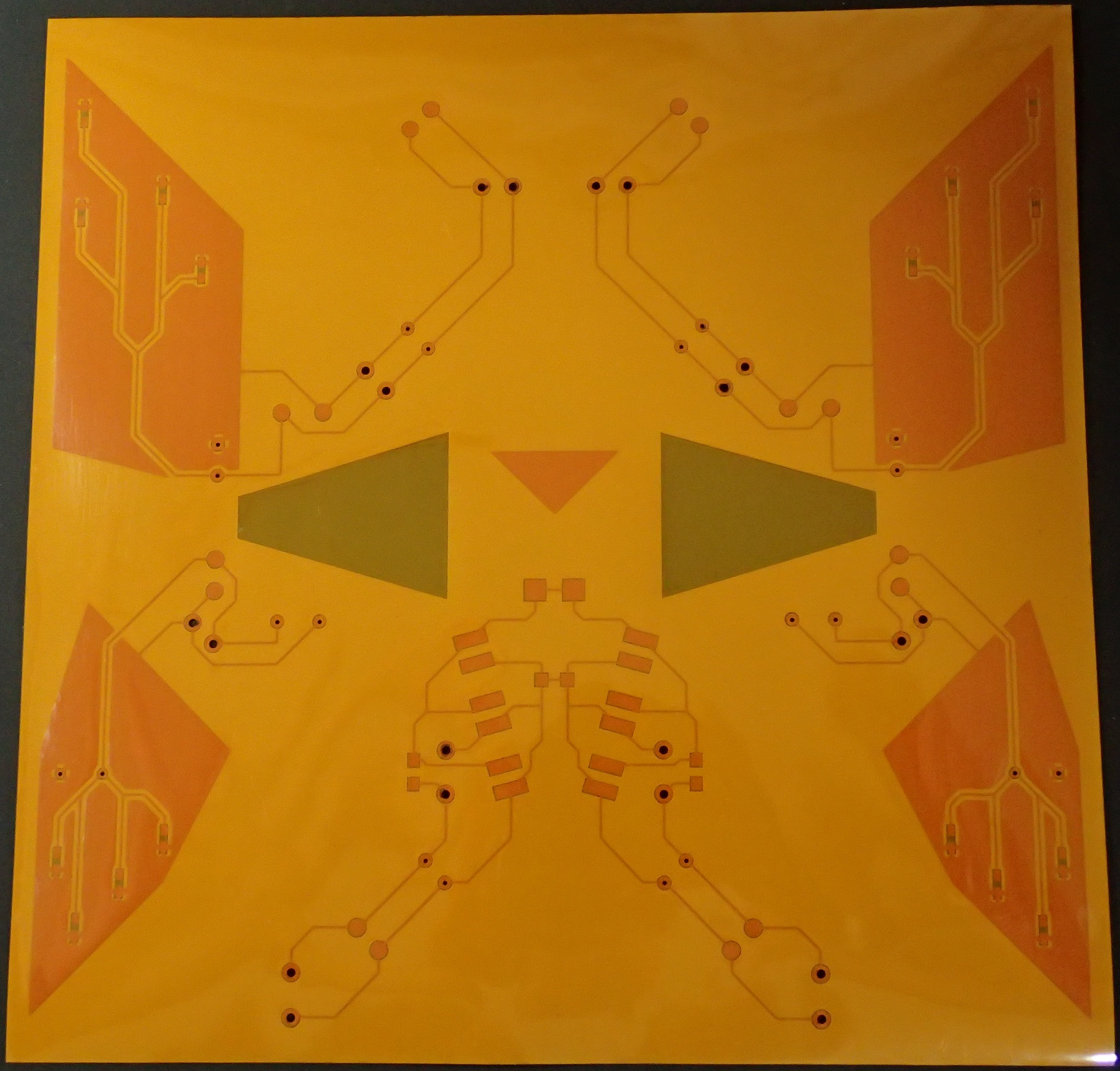

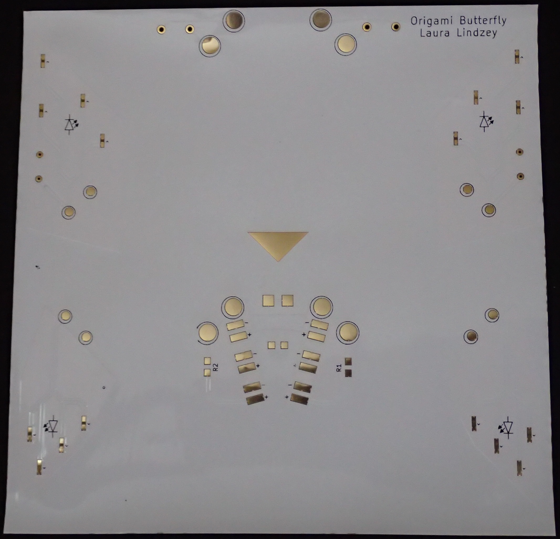
Version 1 of the butterfly PCB. Left: single-layer design as rendered by tracespace; Center: Top of board, as fabricated; Right: bottom of board, as fabricated
For V1 of the design, my gerbers were fabbed as submitted, and everybody was happy. Well, everybody who didn’t try to assemble one. I paid PCBWay $113 for 10 copies of the 125x125mm boards + shipping.
For V2, I was more adventurous with the coverlay mask, and what I submitted first wasn’t feasible to fab. Instead of notifying me of this, PCBWay made several changes to my design without telling me, then sent me the boards. I paid $232 for 20 boards + shipping + a newly-added CC charge.
Version 2 of the butterfly PCB. Left: single-layer design as rendered by tracespace; Center: Top of board, as fabricated; Right: bottom of board, as fabricated
Uh-oh. All of the carefully-drawn masks on the creases were ignored. (They also moved/resized some of the silkscreen around pads and in the LED footprints.)
When I emailed them to ask what had happened and how to fix it, they were willing to re-do my order, for the price of shipping. I still don’t have a super clear idea of what all is (im)possible, and there was a little bit of a language barrier. Thankfully, their customer service rep’s English is better than my almost nonexistent Mandarin. They shared the following images and guidance:
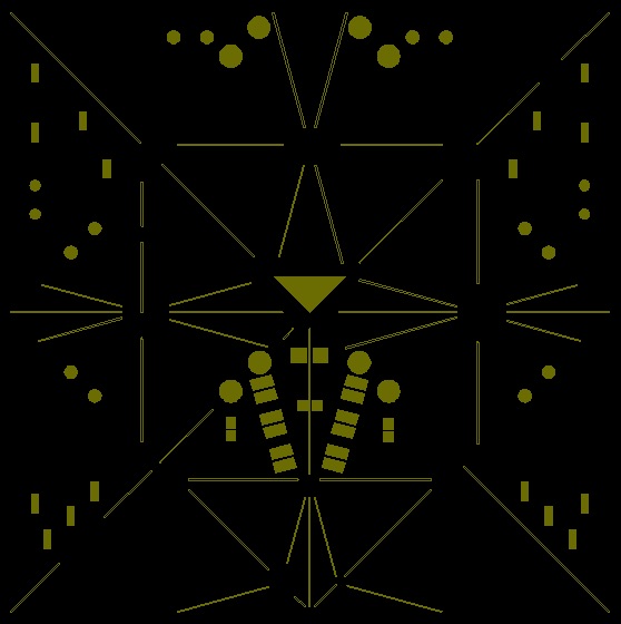
PCBWay’s suggestion for where it was feasible to put coverlay mask. Triangle/circle/rectangle are component footprints, lines are the mask.
As for flexible PCB, is it impossible the produce soldermask opening as line, that will separate the whole PCB but coverlay of fleixble PCB shoule be in a unit and can not separate by line.
For attached pictures, our engineer designed 0.2MM width slots in section and leave at least 8-10MM space between slots. Is this design OK for you?
It really helped that they sent me suggested modifications to my layout; while not quite suitable for my goals, their suggested layout gave me ideas about what was possible. (Lesson: communicate with pictures!)
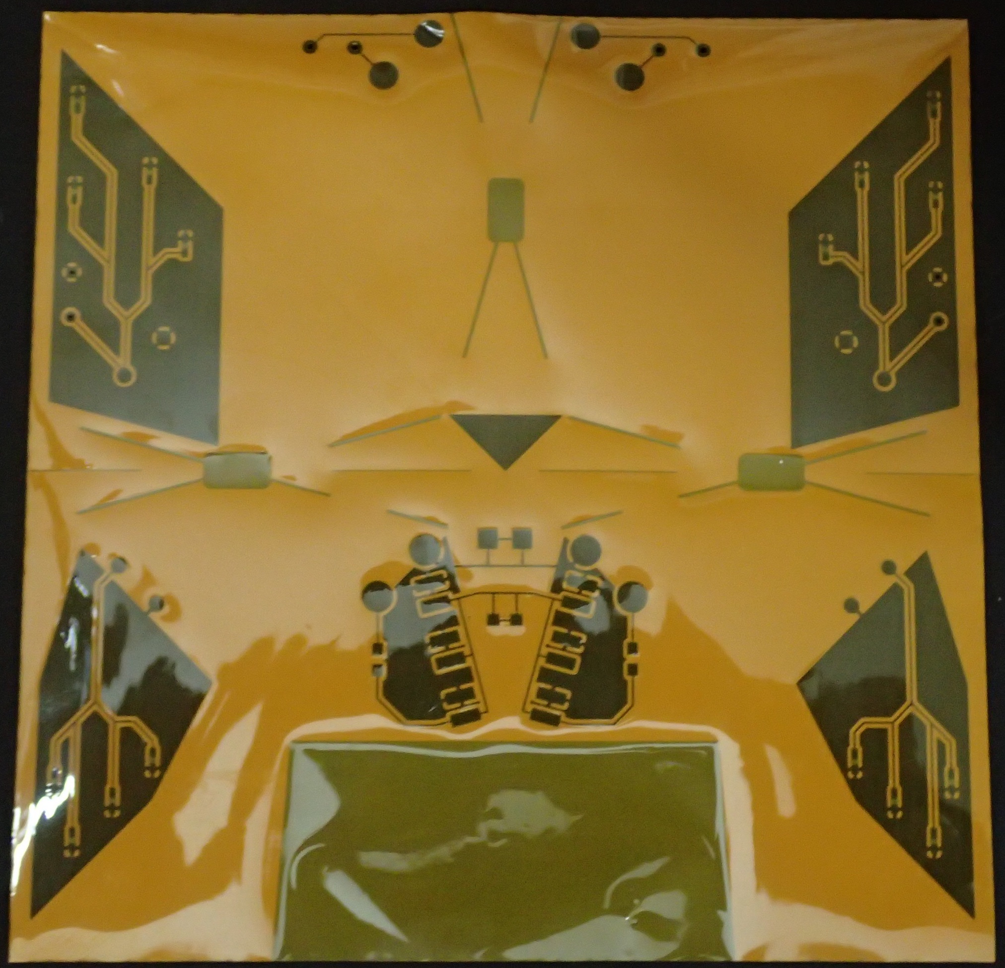
Version 3 of the butterfly PCB. Left: single-layer design as rendered by tracespace; Center: Top of board, as fabricated; Right: bottom of board, as fabricated
I sent back another draft of the layout, and asked if it could be fabricated without modification. This time, it was successful! I paid $26 for shipping.
I’m happy with the quality and customer service I received from PCBWay, and plan to order from them again.
However, it wasn’t perfect ...
The edges of the board have evidence of other silkscreen. I’m not sure if this was a guide for cutting, or somebody else’s design. It’s not a big problem for me, but could be an aesthetic consideration for somebody else.
One of my boards didn’t have some of the coverlay gaps removed (they were cut, but the resulting tab hadn’t been removed). I’m not at all bothered by this since I ordered 20 boards, but received 21.
The alignment was off between the silkscreen and the slots in the coverlay.
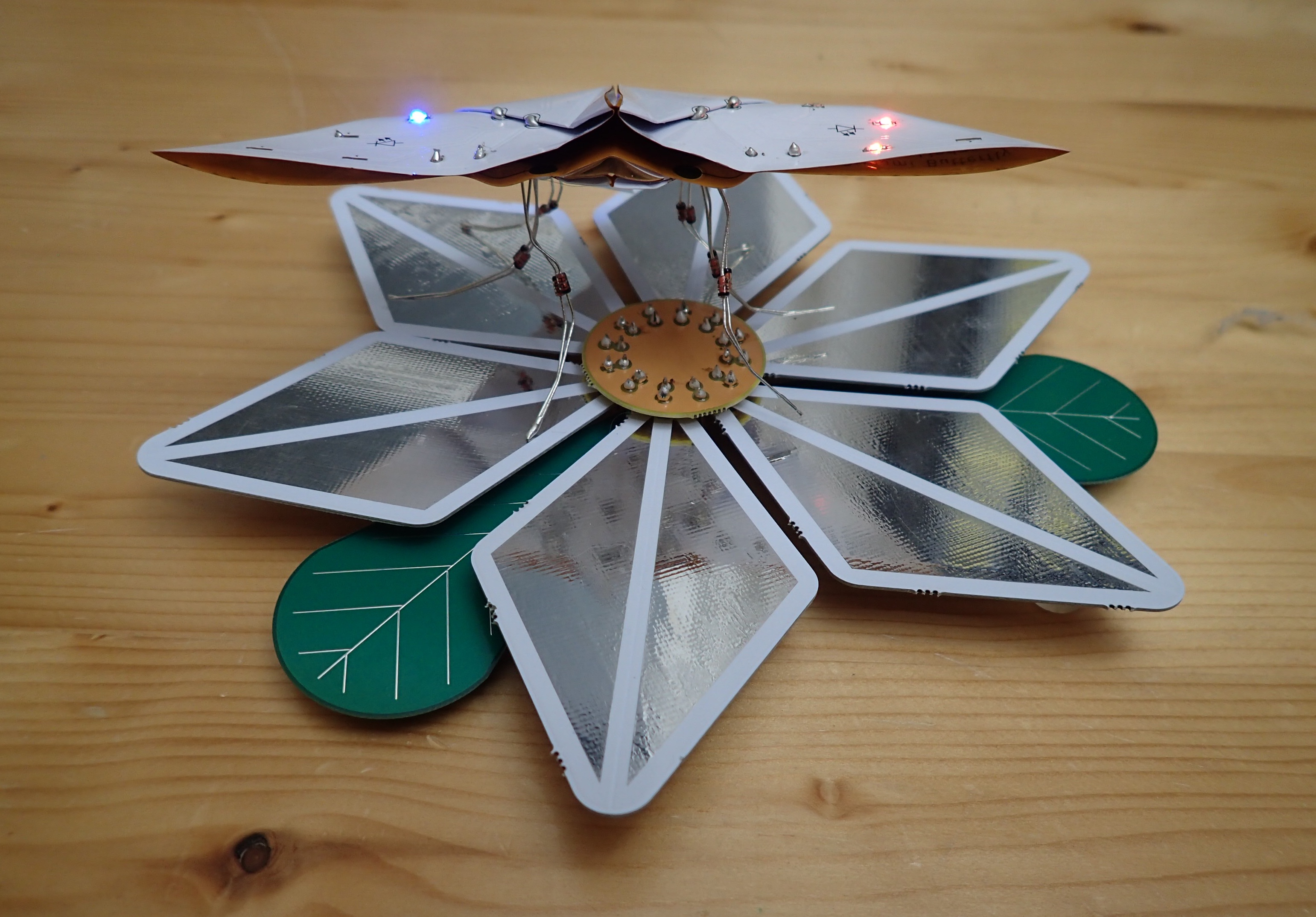
...oh yeah, the flower
For a long time, I just used some copper tape to provide the landing pads to power the butterfly. Ugly, but effective.
Original flower -- made with printer paper, copper tape, and a battery held in place with a binder clip.
Designing the PCB flower was a lot more straightforward, aside from needing to ensure that the different components actually fit together.
So, I scripted it. Hackily.
It turns out that the .kicad_pcb file is plain text with a simple syntax. A few experiments with diffing the files after adding components through the KiCAD pcbnew GUI gave me all I needed to know to write some utility functions for plopping down footprints / lines / polygons. From there, I did all of the geometry by hand and wrote functions that would add petals / leaves / centers to the layout at a given position and rotation.
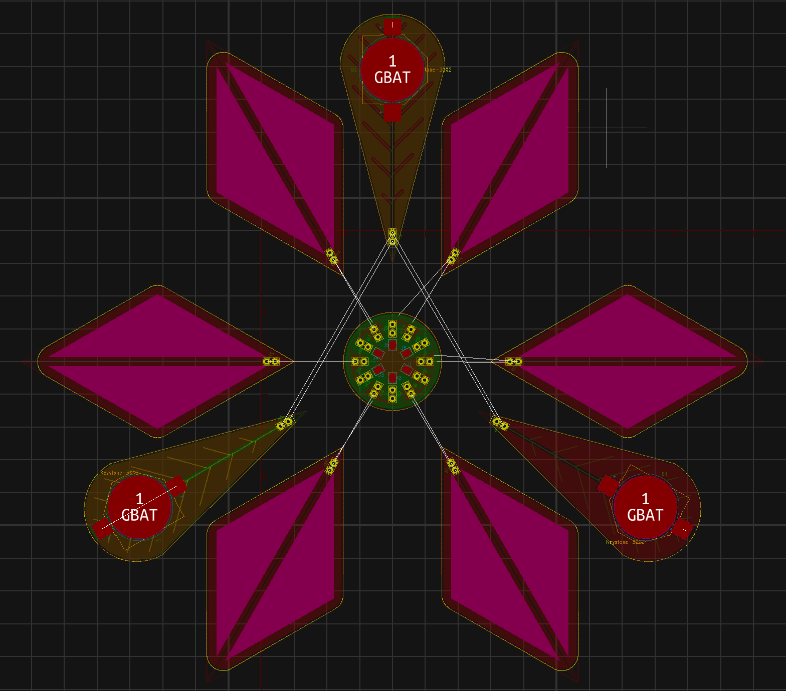
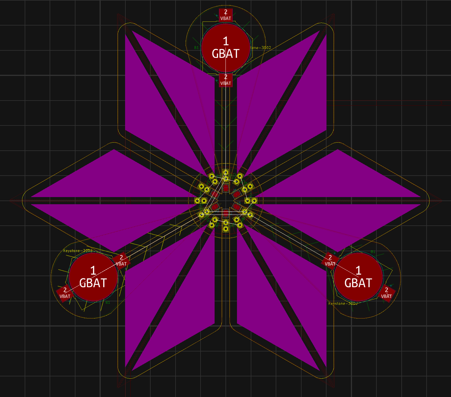
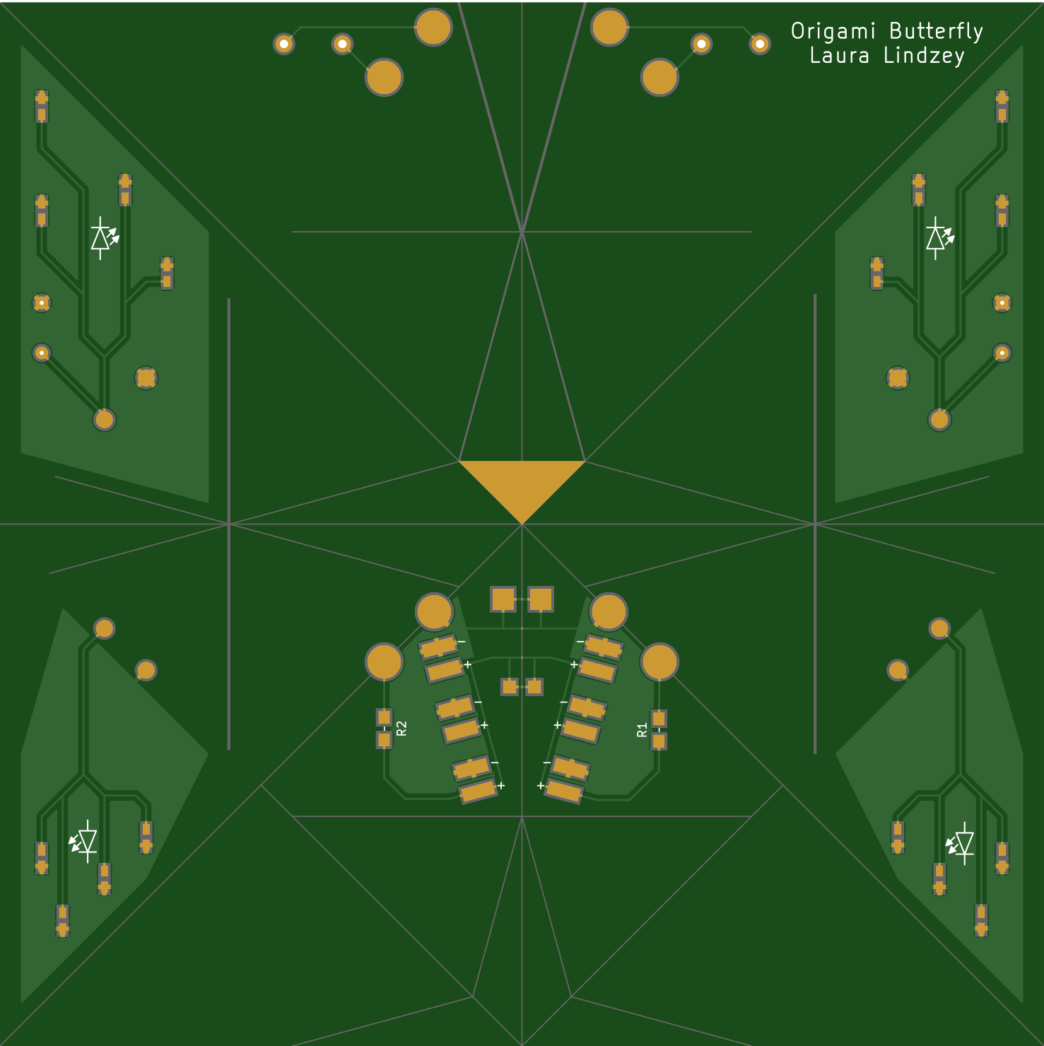
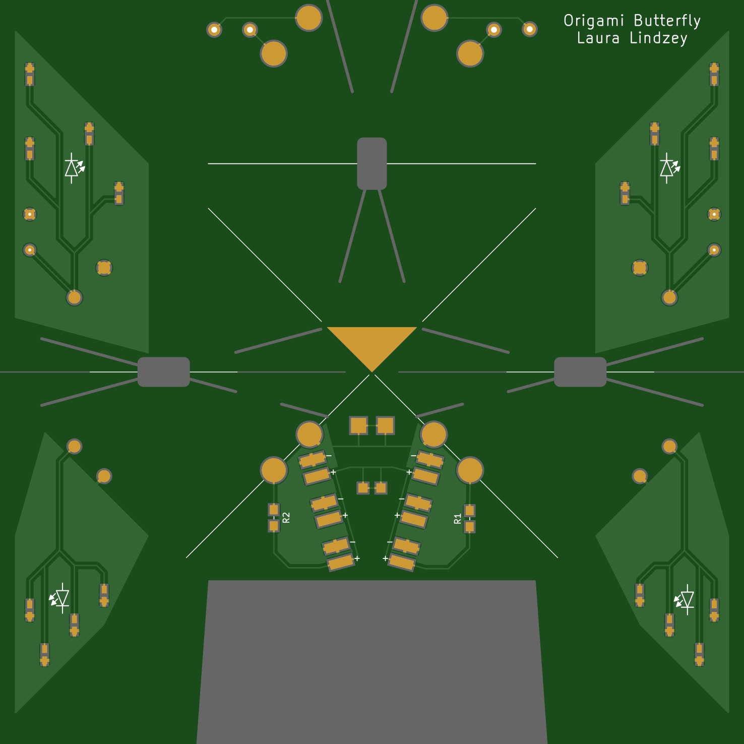
PCB layout displayed in KiCAD. Left: exploded view (with groundplanes filled), Right: stacked view.
This made it easy to generate .kicad_pcb files with the flower both as it would be assembled and in an exploded view. I used the assembled view to make sure it would fit together once I ordered all the pieces, and the exploded view to check that my ground pours were correct (since kicad really doesn’t like computing ground pours in areas with overlapping edge cuts).
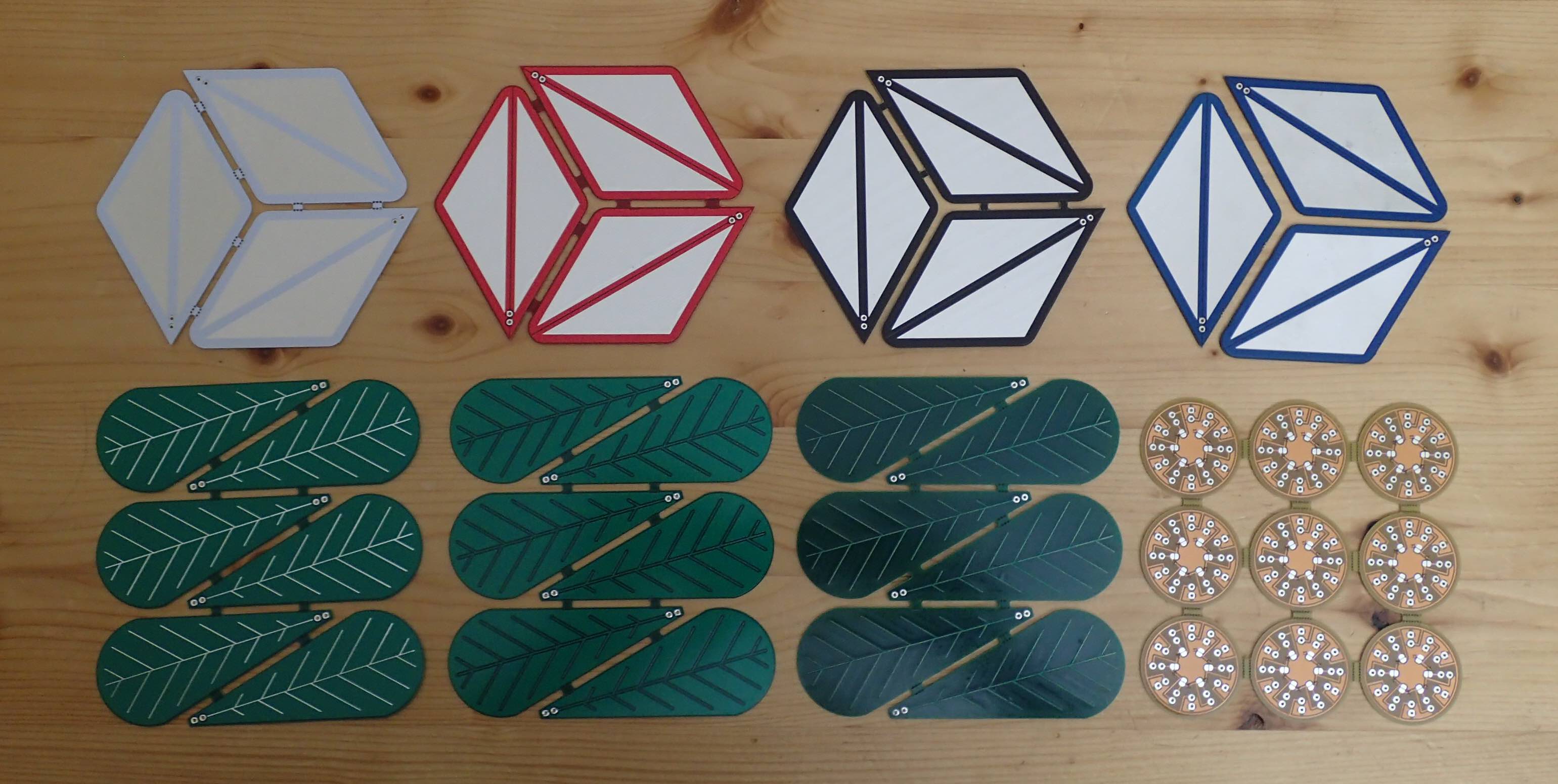
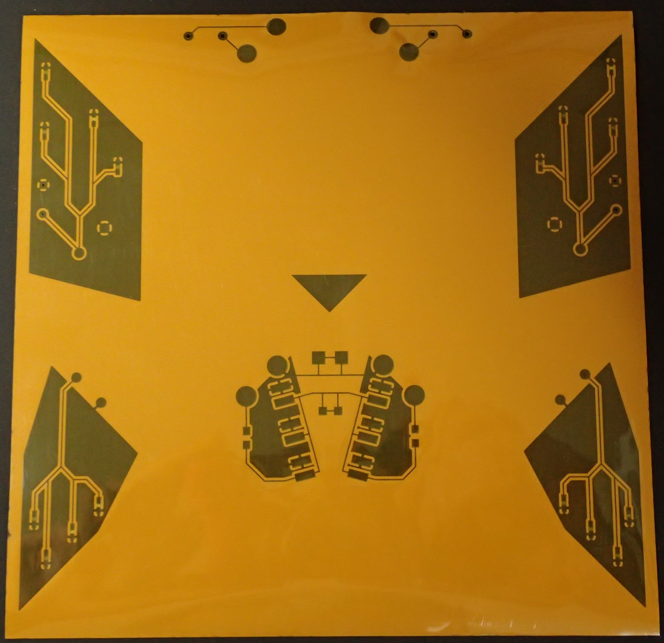
Panelized flower components, as fabricated by Elecrow.
Scripting also made panelization easy!
However, if I ever do something like this again, I’ll try to learn the official KiCAD API.7 My way was far too labor-intensive and fragile.
For standard PCBs, I use Elecrow because they don’t charge extra for panelizing, so long as all components are identical. They did a good job, though if you look closely you’ll see that they changed the mousebites. The petals were all from the same gerbers, but each color was handled slightly differently (black is as-ordered).
I wanted this to be easy to send by mail, so I ordered the flower parts out of 0.6mm thick PCB. It worked! I can fit everything in a standard notecard + envelope, and I haven’t had any reports of them arriving broken.
Finished!
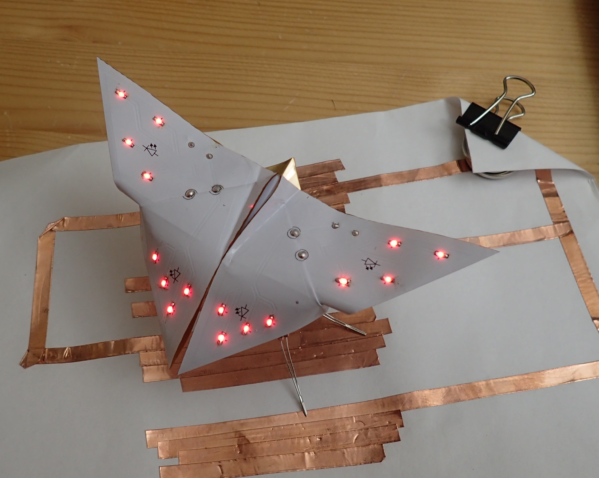
Finished butterfly - you can mix and match LED colors, but each wing (left/right) has to have LEDs with the same voltage drop.<
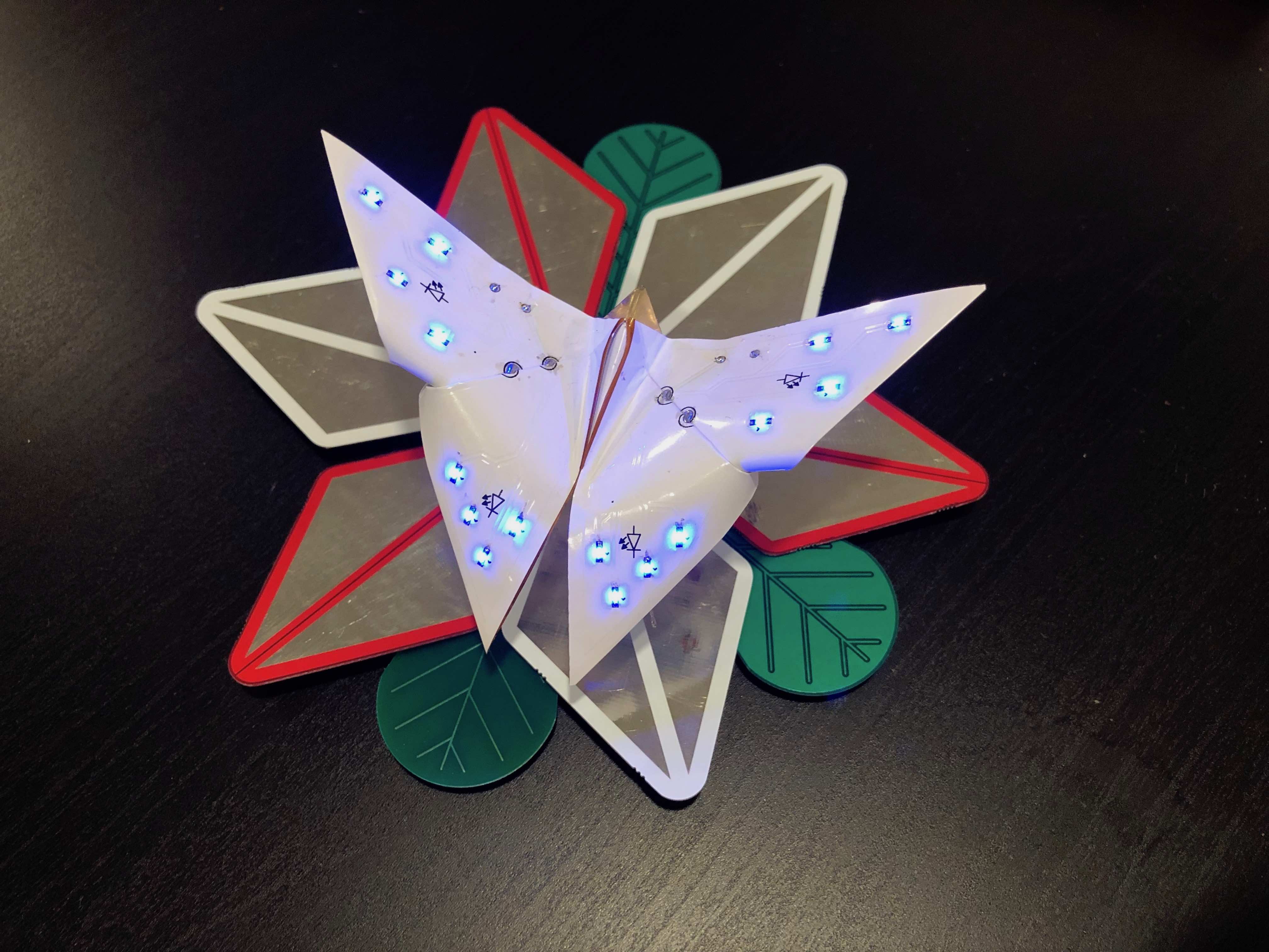
Thanks to Tobin Yehle for being a beta-tester for assembling these and for providing this photo!
Acknowledgements:
If you think this is cool, you should definitely check out Boldport's work; they were a direct inspiration in my new hobby.
Also, I am far from the first person to play with origami circuits — Jie Qi and others in the High Low Tech Group in the MIT media lab have some amazing work.
Thanks to:
- Luke Voss for being an awesome brainstorming partner at the conceptual design stage, and for attempting to assemble a V1 butterfly. Watching how painful it was, I was inspired to try a new way of connecting traces on different facets.
- Boldport Club for the inspiration, and for the discord server of club members who organized this exchange.
- Annie Cherkaev & Tobin Yehle for beta testing the V2 butterfly assembly.
- Annie, Tobin, Wesley, Ben and other members of the Recurse Center remote hardware hack night who provided peer pressure to keep working through the boring bits.
- Googling suggests that this is a slight variation on the classic Yoshizawa butterfly ↩
- I took this idea from all of the absolutely awesome Boldport insects that have legs made out of resistors. ↩
- If I was willing to use black or yellow coverlay, I could have gone thinner (0.08mm), but I thought a white butterfly would be prettier. ↩
- Coverlay serves the same purpose as solder mask and is usually used for flexible PCBs because it doesn't crack when bent. It is a sheet of polyimide that is adhered to the circuit, which imposes additional constraints on design (e.g. the coverlay must be a contiguous layer, you need to design in additional clearance for the adhesive to squeeze out around pads, there is a larger minimum dam size) ↩
- e.g. Oshpark's two-layer specs, Elecrow's specs ↩
- I went with PCBWay, for purely economical reasons. And because I figured if these awesome magnetic actuators were ordered from them, then they couldn't be too bad. ↩
- this seems like a comprehensive guide for where to start scripting kicad with python. ↩