My First PCB!
Designing a PCB1 and sending it off to fab is surprisingly accessible and feels like a super power. I’d been intimidated for years, but finally jumped in. Also, I love living in the future! For <$20, you can design a PCB, have it manufactured in a factory, and get it mailed to you. This still seems insane to me.
This post describes the path I took to get my first PCB manufactured, with an emphasis on not getting sucked into optimizing every decision. I’m assuming you already have a circuit drawn out or breadboarded2, and you want to immortalize it.
I estimate that going from “what is KiCAD even” to ordering your first PCB could be a reasonable one-day project for a simple circuit you already have sketched or breadboarded. It only took me a few days because I was paying a lot of attention to the aesthetics of the board.
My Circuit
While doing a mini batch at the Recurse Center, I became fascinated by the oscillator circuit3 that powered the RC Christmas ornaments. I love how simple the circuit is, while generating visually-interesting behavior!

I wanted to play with varying the frequency of the oscillator by using different values of resistors and capacitors, so I made a protoboard wired up with female header to make this easy. It turns out that LED color also makes a difference! I dislike breadboarding for anything more extended than a proof-of-concept (it is the physical incarnation of spaghetti code) and protoboard4 can be a pain to work with. So, I figured an oscillator circuit with female headers for all of the components could be a fun first PCB to have fabricated.
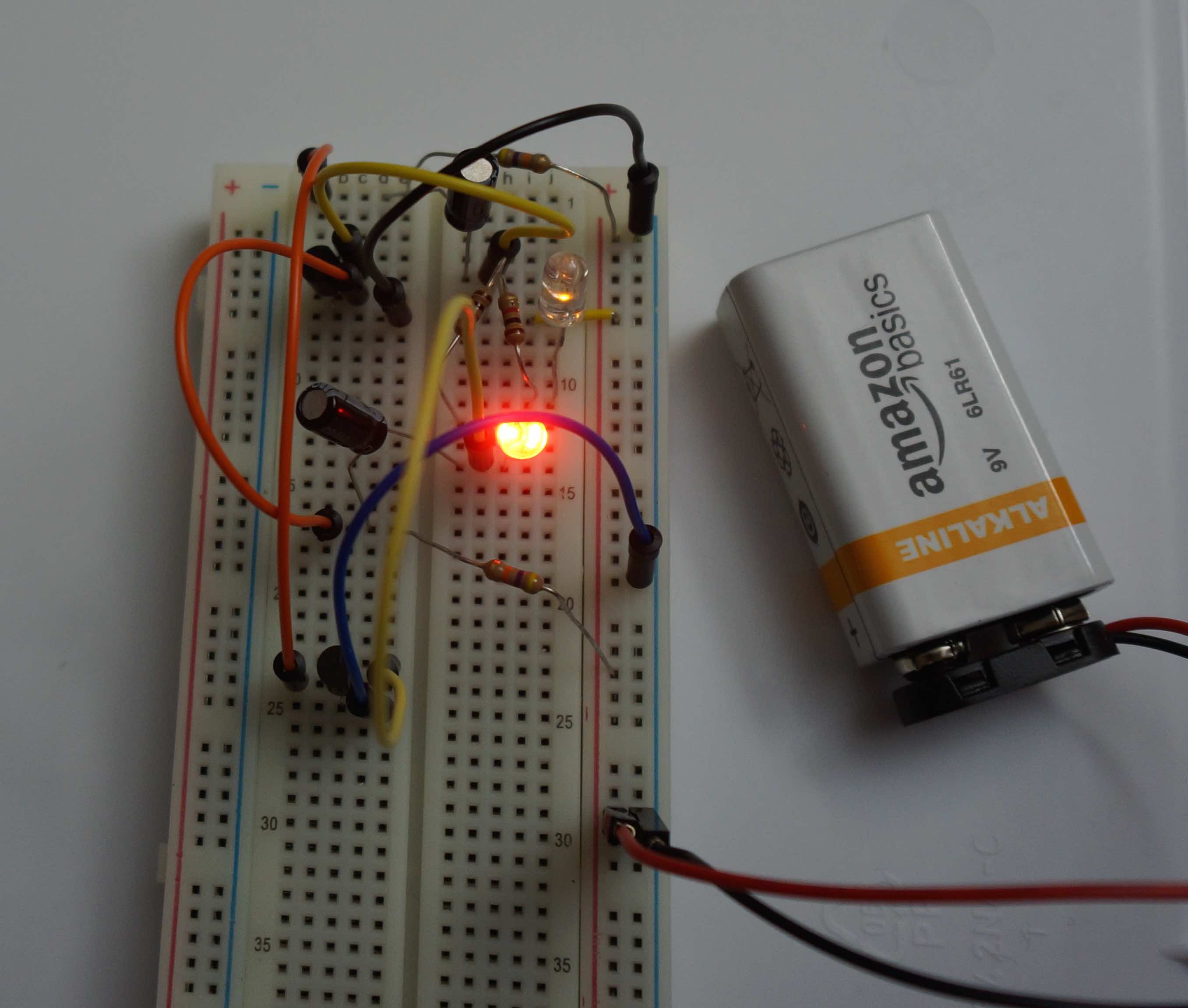
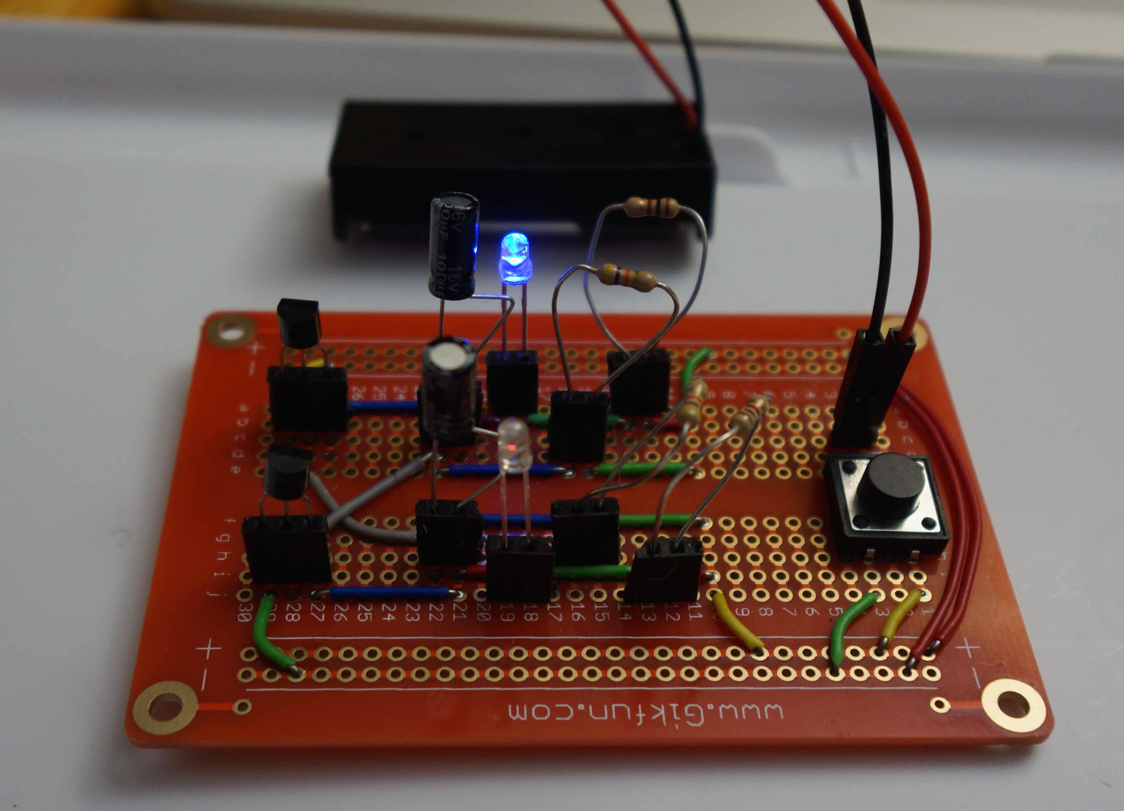
Early implementations of the oscillator. Left: on breadboard, Right: on protoboard.
CAD tool for PCBs
I really like KiCAD5 as a design tool because it decouples documenting the circuit logically from laying it out on a board. This is great for when I want to have professional-ish schematics of things that I’m only ever going to implement in protoboard. I think Eagle is the main competitor, but it has a tight coupling between the logical schematic and the physical layout that forced me to care about component packaging and footprints way too early (like 2 years too early), so I bailed on it quickly.
Plus, KiCAD is open-source, which makes me happy.
There are 3 primary phases to designing a PCB in KiCAD:
- Use EESCHEMA to generate a schematic for your circuit. This will be a digital version of the hand-drawn circuit from above.
- Use CVPCB to associate each element in the schematic with a specific component’s footprint. For example, resistors come in many shapes and sizes, and before laying out a PCB, you need to choose which resistor to use. The footprint specifies its physical size, connections to the board, silkscreened outline, and sometimes even 3D view.
- Use PCBNEW to define the board’s boundary, arrange the footprints on the board, add traces connecting components, and add annotations that will be silkscreened.
This video tutorial by Widsor Schmidt was well done. He walks you through the whole process (opening KiCAD for the first time to finished PCB layout) in 20 minutes. I watched it repeatedly on 2x speed, pausing so I could follow along.
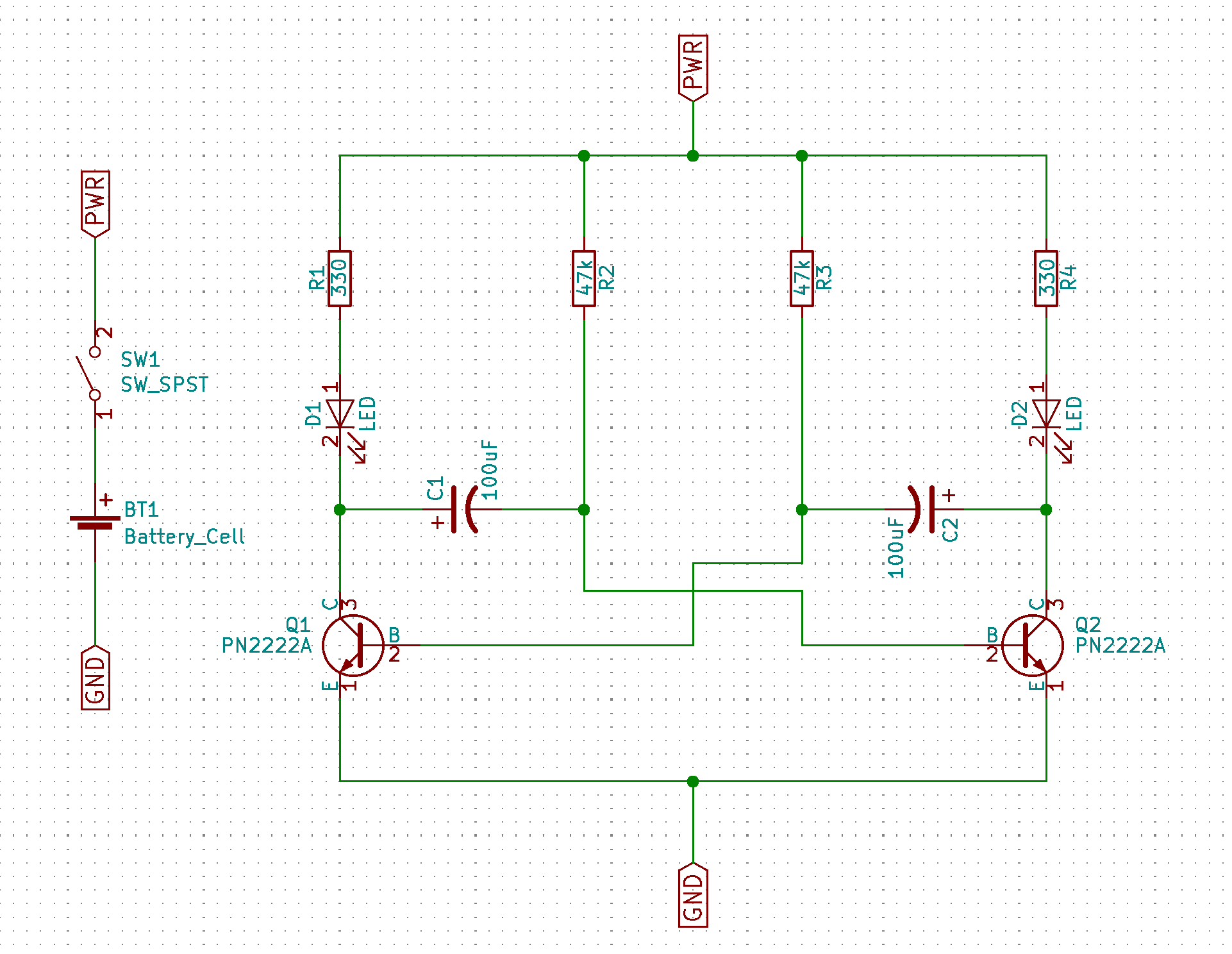
Schematic
I don’t remember what tutorials I used for learning how to set up a schematic using KiCAD’s EESCHEMA program, but Schmidt’s video also covers that. I first used it a few years ago, and recall that I spent an evening to go from “KiCAD seems interesting” to “hand-sketched emergency stop schematic for my robot is now laid out nicely”. Here’s my oscillator circuit as represented in EESCHEMA:
Component Selection
Next, we need to associate the symbols on the schematic with a real-world component that matches the required specs. This requires both picking the actual components you’ll use during assembly and specifying the footprint they need on the board.
If you want to use components that aren’t in one of KiCAD’s built-in libraries, you can make your own footprint. I’ll have to learn this eventually, but since my plan was to solder female headers to the board so I could swap components out, this was irrelevant. To save time on your first board, you can just use through-hole components with bendable leads (which you probably already have from breadboarding!) or footprints that are already in the libraries. If you’re desperate/lazy, just use the footprints from the connector library -- they’ll work for anything that you were able to use on a 0.1” pitch breadboard!
The exceptions to this are the power switch and battery, both of which took me a long time to find and aren’t part of a typical breadboarding kit. I passionately hate Digikey’s search interface. It is shockingly bad at having the right metadata for filtering to be effective. Mouser is sometimes better, but I'm still not a fan. So, here are some good-enough options:
- I used these breadboard-friendly switches from Sparkfun. I also like the C&K JS202011CQN, which has a footprint in the KiCAD Button_Switch_THT library.
- I used a coin cell battery to power my project. There are KiCAD footprints for the Keystone 3000 (12mm) battery holder and Keystone 3008 (24mm). I prefer the Harwin S8211-46R for a 20mm battery because it’s easier to get the battery in/out, but there isn’t a built-in KiCAD footprint.
If you want to scale down components to make the final board smaller, you’ll have to spend time shopping ... and scaling down in size also means figuring out how to do surface-mount soldering with tiny components. I may get to that someday, but not yet.
Board Layout
The next step was to lay out my circuit as it would appear on a PCB.
I fiddled with the layout a lot (entirely redoing it 3x), and had lots of drudgery figuring out how to get the silkscreening to look almost right. I still don’t have a process that I love for that ... I imported public domain electrical symbols as bitmaps, but it was hard to get their leads to have the exact same width to match.
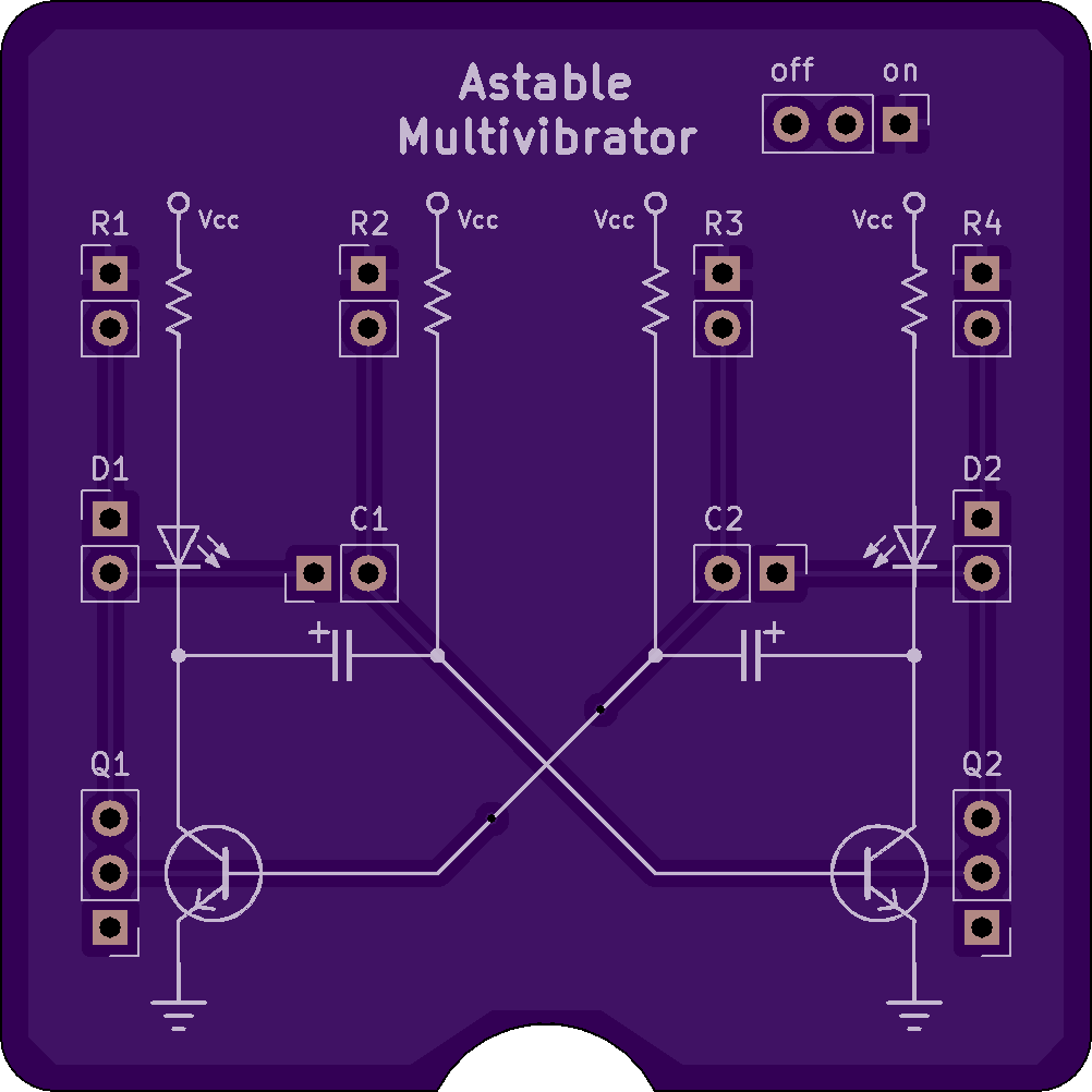
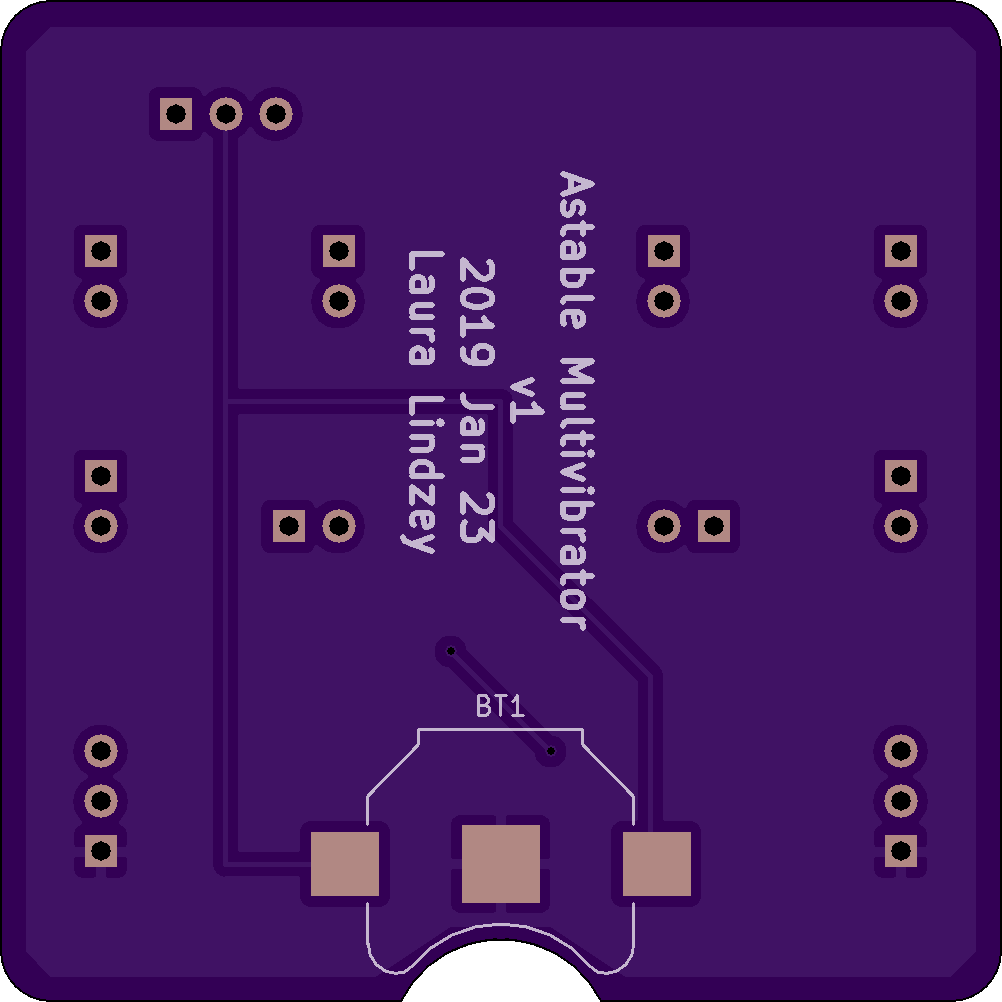
Here's the representation of my board from pcbnew, showing all of the layers at once:
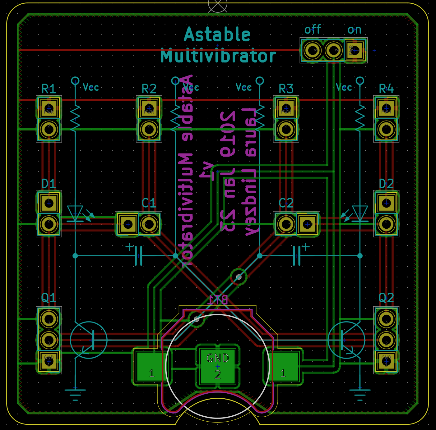
I don’t remember when/how I came up with the idea for making the circuit diagram part of the PCB design, but I suspect it was influenced by having seen Star Simpson’s Circuit Classics6 at some point.
Fabrication
Once you’re happy with the circuit layout, head over to OSHPark and upload your kicad_pcb file. Their interface is fantastic, and provides a nice rendering for you to do a final check on each layer, in addition to what the whole stackup will look like when manufactured:
Renderings of the front (left) and back (right) of my PCB, generated by OSHPark.
I didn't spec out the full market of available fabricators because OSHPark hit a sweet spot for me at the intersection of "cheap enough to do on a whim" and "caters to hobbyists/small batches, plays exceedingly well with KiCAD”, with a bonus of “the EE at work uses them for custom boards for our several million dollar robot, so quality must be OK”. Seriously, actually placing the order was the easiest part of this whole process. Their automatic import (straight from KiCAD’s .kicad_pcb format) automagically worked.
My first version of the layout was going to cost $7.85 to get 3 copies of the board. I made it bigger for aesthetic reasons, so I wound up spending $20.05, and shipping is free.
Results!!
OSHPark did a great job, and they’re prettier than I expected!
I assembled two out of the three -- one with header7 so I can swap in and out different components, and one with blue LEDs tuned to flash at about 1 Hz.
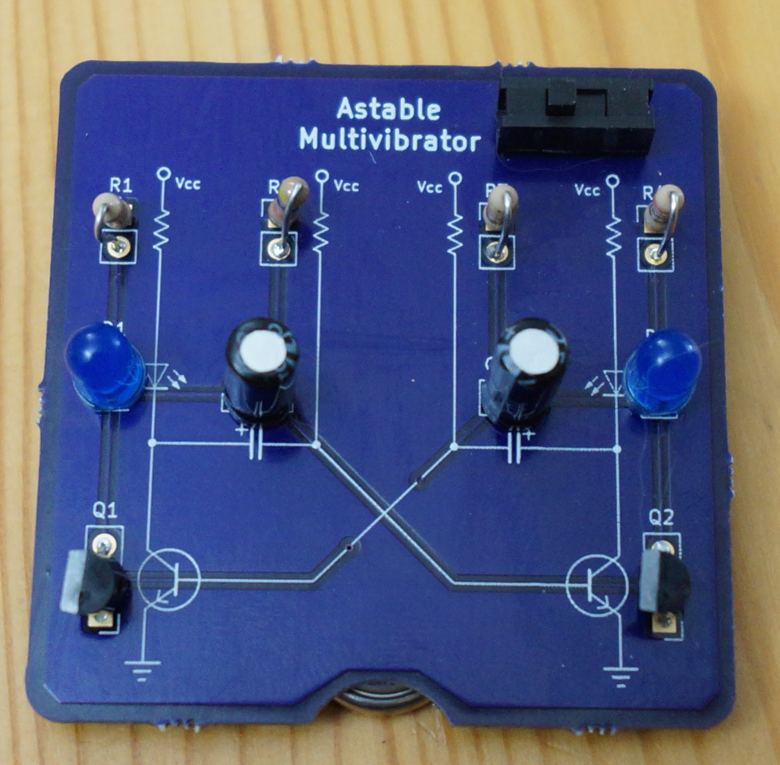
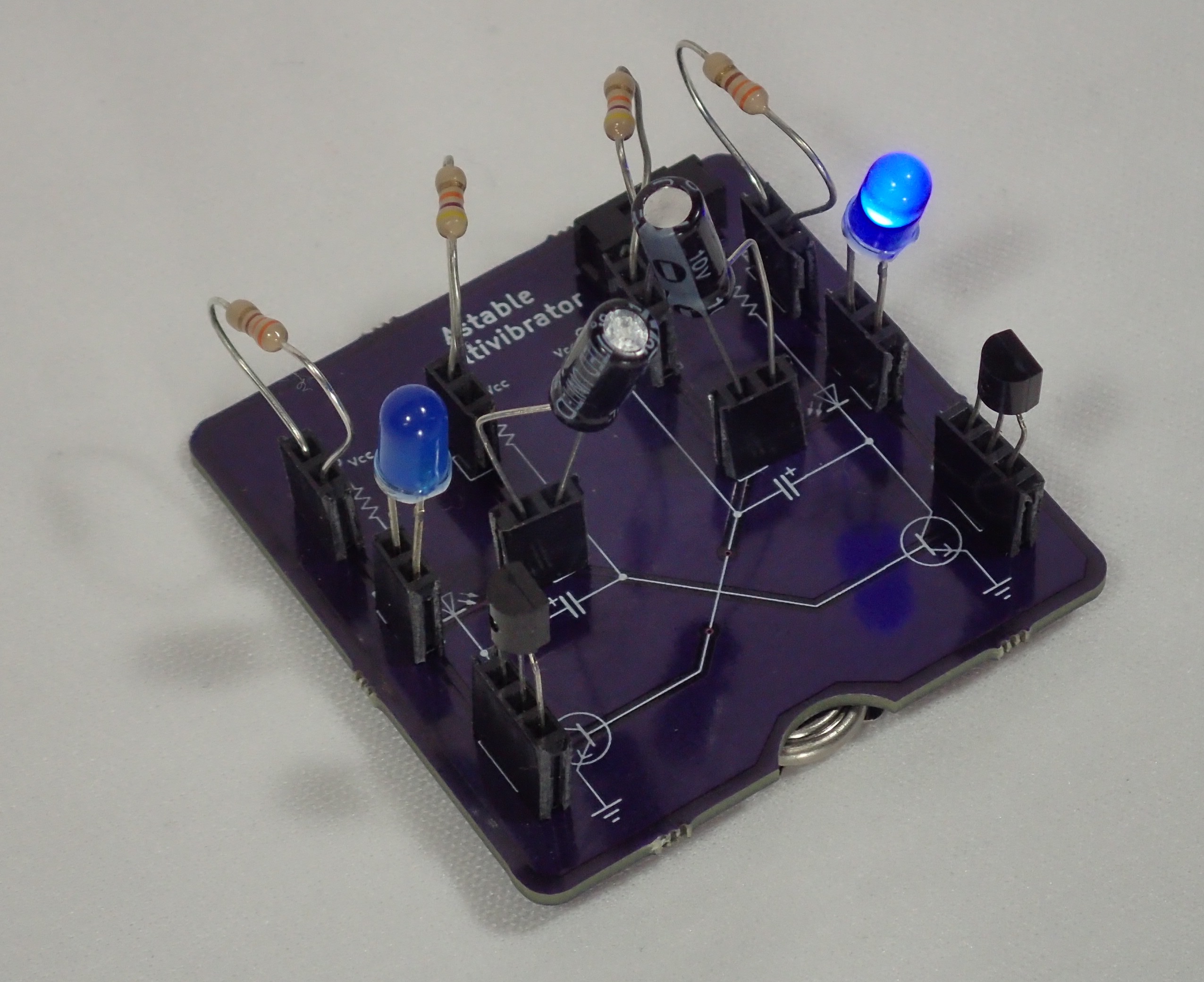
Assembled boards!
The rough bits around the edges are mousebites, which are added by OSHPark in order to attach my board to others during the fabrication process. Afterwards, the thin tabs break easily, separating the boards. I don’t really want to sand fiberglass, so I may try covering them with clear nail polish.
There are a few issues that I'd fix in a v2:
- One of the vias is under the battery, and for some reason, it isn't covered with solder mask. Given that it's a bit recessed, it probably wouldn't have made contact, but to be safe, I put down a piece of kaptan tape. I think “tented via” may be the right keyword here?
- The negative battery pad is also recessed, and the battery isn't making contact. For now, I applied a bit of solder to raise it up. I think the real fix may be to re-design the battery footprint such that the central pad is bigger and/or has a wider border of no-copper around it.
- My LEDs don't turn off as quickly as the RC ornament one did. This has nothing to do with PCB design, and everything with me not yet fully understanding how different components affect the circuit. The header test board is meant to make testing my understanding easier!
However, I’m pretty happy with this! While I still have lots to learn, the workflow seems solid. My next step will be figuring out how to add my own footprints so I can use any component I want.
Acknowledgements: Huge thanks to the community at RC for inspiring both the project and the writeup! Aaron Strick & Noah Zachary Gordon provided the original inspiration and encouragement to post this. Veronica Hanus & Robert Schuessler commented on an earlier draft.
- A Printed Circuit Board (PCB) provides places to attach the components in your circuit (pads/footprints) and provides the required electrical connections between them (traces). ↩
- If you need inspiration, how about a LED that lights up when you push a button, or a LED that turns on in the dark? Or, check out the 100 simple circuits in the back of Forrest Mims's "Getting Started in Electronics". ↩
- These are lots of websites explaining how this works. Here's a nice simulation, and here's a simpler explanation. ↩
- I'm always frustrated by the awkward layout and the fiddly solder bridges protoboard requires. However, it's useful if you want to make a breadboarded circuit more permanent without actually making a PCB. If you have to use protoboard, I like these from gikfun because they have the same electrical connectivity as a breadboard. (Adafruit's perma-proto is also good, but more expensive.) You can't get the layout as dense as you can on other protoboard, but it cuts down on how many solder bridges you have to create. ↩
- I used v4 for this project, but you should definitely use v5. They fixed a lot of the rough edges, and it's more pleasant all-around. ↩
- I was chagrined to rediscover her work while halfway through this project, and then realize that she actually did this exact same circuit! Our implementations wound up being rather different, but I did use her idea for a battery cutout. ↩
- For this build, I used standard female header, cut apart with my wirecutters. It didn't work very well. In addition to being ugly, the components fit loosely. Next time, I'll use machine pin header, which provides a tighter fit for component leads and comes in a breakaway version even for female header. ↩